MICROSECTION / CROSS-SECTION ANALYSIS of PCBA and BGA
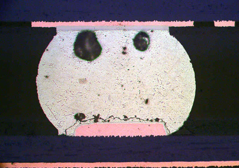
ross sections reveal defects and features of circuit assemblies that may not be detectable or measureable using non-destructive methods such as X-ray, CT, or optical inspection. Microsectioning shows intermetallic (IMC) layers, solder defects, and other physical characteristics of surface mount devices, such as BGA's, LGA's, and bottom terminated QFP's, as well as PCB inner layers and construction. PSI uses microsection for both failure analysis and validation of assembly processes.
PSI works with you to determine the ideal plane(s) for sectioning, taking into account board characteristics, failure mode, and X-ray observations. Wherever possible, additional planes of interest are preserved for potential future investigation. Samples are excised from the board, potted in a special epoxy, then polished and etched to expose the desired plane. PSI's experienced technicians use a carefully refined polishing process to yield a smooth finish that preserves fine details, such as grain structure and intermetallic layers, and minimizes scratches and artifacts.
Circuit Assembly Cross Section examples:
FAILURE ANALYSIS - BGAs & PCBAs
Whether you're grappling with field failures or ornery prototypes, PSI can help you get to the bottom of your SMT related failures. Cross-sectioning allows PSI to isolate and characterize failure modes such as fractures, delamination, PTH plating integrity, and poor solderability. Sectioned samples can also be viewed using our Scanning Electron Microscope (SEM) or Energy Dispersive X-ray Spectroscopy (EDS) equipment, for ultra high magnification inspection and/or elemental analysis. Even if your failure turns out to be other than attachment related, PSI can help you rule out SMT problems, steering your search toward the real culprit.

Quality matters. A PSI client was experiencing delamination of PCBs produced by an offshore fab, while identical samples from their domestic supplier did not have this issue. One sample from each fab was submitted for micro-sectional analysis. Barrel cross sections are shown above @ 500x. Left: The sample on the left is from the offshore fab. Nailheading, rough edges, and delamination (not shown here) of the outer copper layer all suggest poor drilling and deficiencies in the materials or stackup process. Right: The sample section on the right was produced from the same board artwork, but by a US fab.

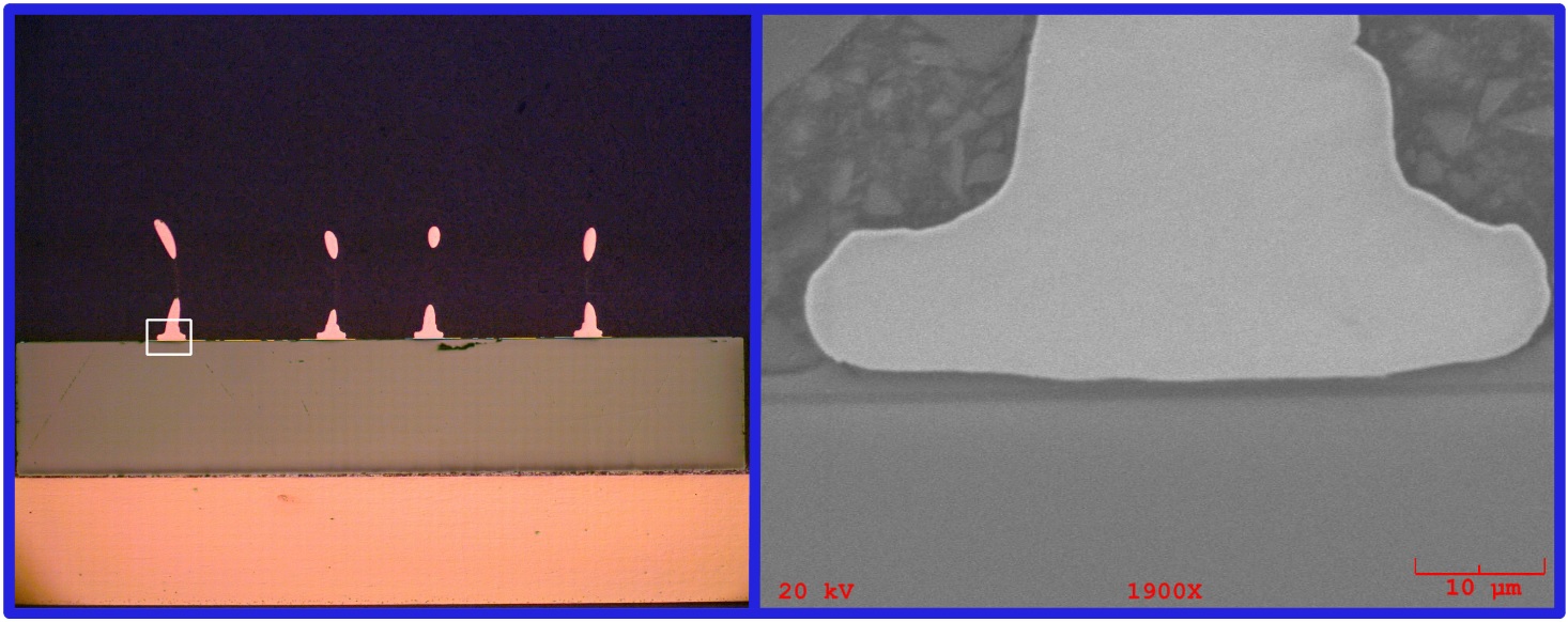
Cross-section of die wire bonds, shown @ 100x and 1900x. Image at right was captured on PSI's Jeol JSM-5610 scanning electron microscope.
SMT PROCESS VALIDATION
Don't just wonder whether your process is working. PSI can verifty proper intermetallic layer and fillet formation, fulfilling an essential aspect of your test and validation model. With X-ray inspection and micro-sectioning, PSI can provide evidence of reliability for process validation.
When you need to know, contact the solder experts at Process Sciences.
Microsection | Cross Section | PCBA Analysis | BGA Analysis | BGA crack | BGA fracture


