SMT Failure Analysis
ailure analysis can take you in many directions, with widely varying costs and results. It helps to have a partner who can help navigate the many options available, and weigh the benefits of each. By outlining an analysis strategy that narrows the potential root causes, minimizes cost, and preserves your sample(s) for future analysis when possible, PSI can help you get to the bottom of your investigation quickly and efficiently, with meaningful results. PSI offers:
- PCB & BGA Failure Analysis
- Process Validation
- Real Time, Off-axis X-Ray Inspection
- CT X-ray Analysis with 3D Volume Reconstruction
- IC Counterfeit Detection
- Chemical Analysis
- Solderability Testing
- Mechanical Testing
- Material Qualification
SMT Process Validation
While PSI specializes in failure analysis, we also use X-ray inspection, microsectioning, dye & pry test, and other means to confirm SMT processes, and bring to light anomalies, process indicators, and defects. With over 75 combined years experience in SMT problem solving, our staff of knowledgable analysts, technicians, and engineers can help you overcome any SMT challenge.
Example: X-ray Investigation of BGA sphere volume variation
| {youtube}EA68uIt6V2U{/youtube} |
| There are no defects under this BGA, but a process problem is clearly evident. Typical solder joints are spherical or ovoid, however a large number of the joints in this video look like an hourglass. This shape can result from either a high standoff height, or from significant variations in solder volume. In the above case, the distribution of these skinny-waisted solder joints is random, not concentrated, which rules out warping or non-coplanarity as possible causes. These anomalies must be related to lack of solder volume. Varying solder volume, in turn, can result from paste print variations, missing mask, or BGA component problems. When there is damaged or missing mask, molten solder can wick along the trace during reflow, and sometimes even down a via. (It is not uncommon for the entire solder joint to be "lost" in this way.) However, with neither stray solder nor filled vias evident in this video, it's clear that we are not witnessing solder migration; instead the "missing" solder probably resulted from variations in the paste print. This customer should review their paste storage and handling practices, their stencil design, equipment, and printing procedures, to see why paste was not uniformly distributed prior to BGA placement. |
Analytical Methods & Equipment:
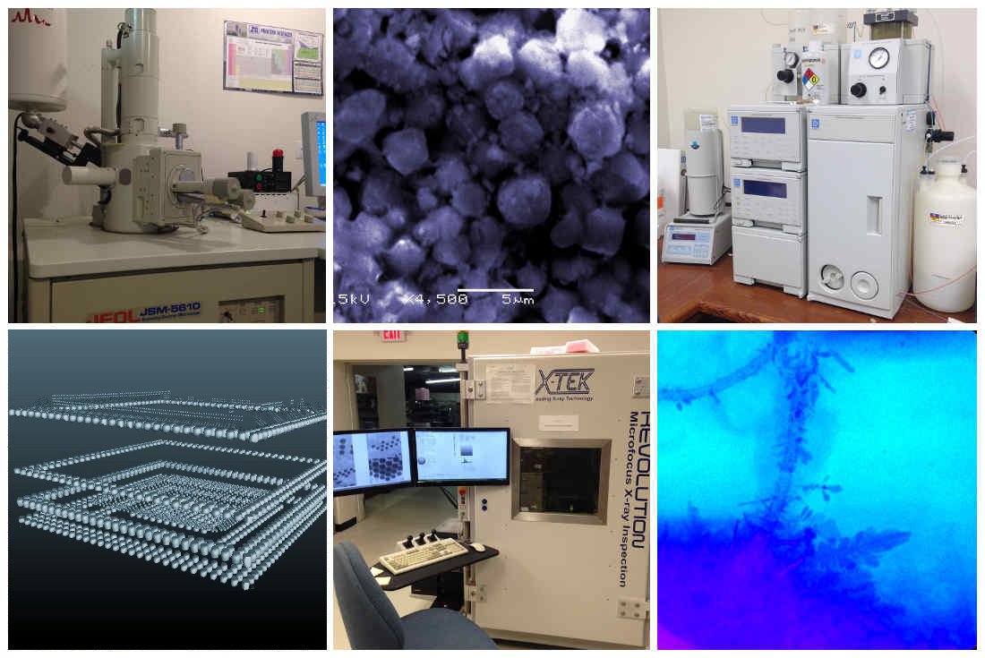
SEM - Microscopy
• Keyence VHX-6000 Digital Microscope
• JEOL JSM 5800 LV w/IXRF EDS 30x - 60,000x
• JOEL JSM 5610 w/IXRF EDS and XRF X-Ray source 30x - 60,000x
• Zeiss Axioskop 2 Metallurgical Microscope 50x – 1000x magnification
• Zeiss Axiovert 200 MAT Microscope 50x – 1000x magnification
Non-destructive Analysis
• X-Tek Revolution Off-axis X-Ray Inspection
• X-Tek XT V 160 CT X-ray System, with 3D volume reconstruction
• X-Tek XT H 225 CT X-ray System, with 3D volume reconstruction
• Dionex Ion Chromatograph / HPLC
• Foresite C3 ion chromatography, with localized extraction
Destructive Analysis
• Cross-sectioning / Microsectioning
• Tensile and Shear Force Testing
• Dye and Pry
Chemical Analysis
• Dionex Ion Chromatograph / HPLC
• IXRF EDS / XRF System w/fx SEM X-Ray Source
failure analysis lab, SMT failure analysis, BGA failure analysis, electronics failure analysis


